Carrier board
The single-chip design runs on a MyIR Z-Turn Zynq-7020 SOM. The carrier board is the custom PCB the SOM plugs into — it turns the core into a real Atari-XT machine by bringing out the Atari-facing I/O the SOM doesn’t have: the SIO port, cartridge slot, the PBI / expansion bus, joysticks, audio in/out, and USB for keyboard and mouse. The carrier is 3.3 V throughout; the few genuinely 5 V Atari ports are level-shifted at their connectors.
The STM32F411 I/O companion
Section titled “The STM32F411 I/O companion”Slow, real-time, “host-the-outside-world” jobs don’t belong in FPGA fabric, so the carrier carries an STM32F411 as an I/O companion. It handles:
- USB host for HID keyboard and mouse,
- SIO host controller — drives the real Atari SIO DIN port, plus virtual disk / network peripherals in firmware,
- Joysticks and paddles — paddles read as RC charge-time on digital pins via timer input-capture, exactly like the real Atari (no ADC involved),
- MIDI — opto-isolated IN, current-loop OUT.
It links to the FPGA over SPI (~5 MHz) plus a few GPIO, with a UART on PS MIO for firmware programming and runtime control. Because the emulated POKEY is register-level (no bit shifter), SIO bytes cross that link as bytes — there’s no UART between the FPGA and the STM32.
Why STM32F411 for USB host, not the RP2354
Section titled “Why STM32F411 for USB host, not the RP2354”The earlier plan used an RP2354 for the USB-HID host. That role moved to the STM32F411 for one decisive reason: host-mode USB is far more battle-tested there. The F411’s USB-OTG-FS controller together with ST’s USB Host library is a mature, widely-deployed host stack, whereas TinyUSB on the RP2350 / RP2354 family is device-mode-first — its host support is newer and less proven. Enumerating arbitrary keyboards, mice, and hubs is exactly the kind of fiddly, edge-case-ridden job where the better-trodden stack wins, so the STM32 takes it.
The RP2354 isn’t gone, though — it just moved to where it shines: each expansion card is an RP2354, using its PIO to talk the carrier’s byte-wide bus (below).
Expansion bus
Section titled “Expansion bus”Every expansion slot carries two interfaces:
- a faithful 1090-style parallel PBI bus (for PBI-shaped cards, via a level-shifting riser), and
- a modern FPGA-direct byte-wide synchronous bus — 8-bit data + clock at 25 MHz (≈ 25 MB/s), plus a 1 Mbit control UART, CS-selected one card at a time.
The byte-bus is single-ended 3.3 V and deliberately slow, so a “fast” card needs no FPGA — an RP2354 + PIO drives it directly while its two cores run the card’s device firmware. The motivating use case is an ACSI / SCSI hard disk behind an ST/TT emulation, where 25 MB/s is roughly twice what a period disk driver needs.
A PCM1808 stereo I²S ADC provides line-in and sampling, and captures the Atari SIO and
cart / PBI AUDIO_IN lines; POKEY’s output rides out over the HDMI link. See
Audio.
A single AP2112K LDO supplies the 3.3 V rail — STM32F411, the USB-hub logic, the PCM1808 digital side, the bus decoder, and glue — comfortably within its 600 mA budget.
The PCB is designed to fit into a reduced-size Atari-TT/Atari MegaSTE style case…
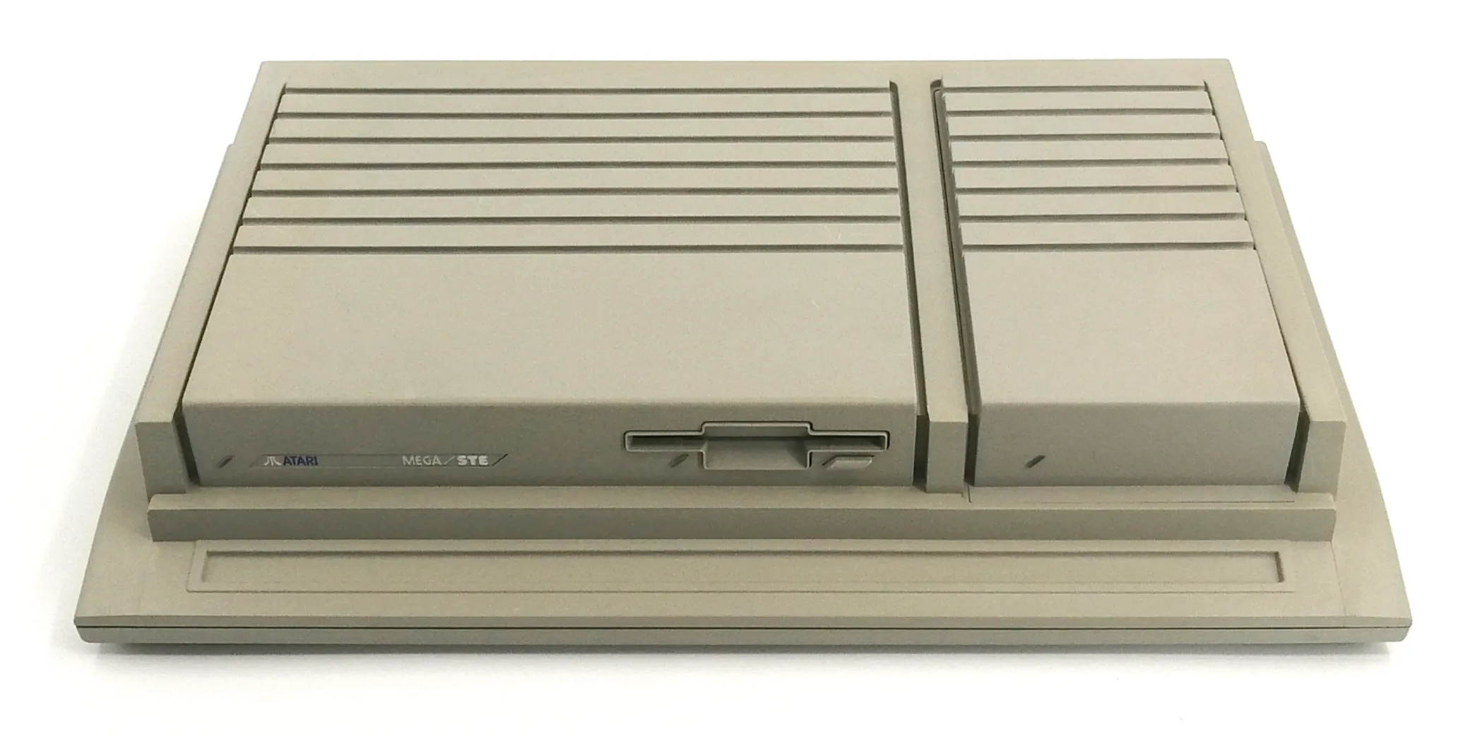
I always thought this was the best case that Atari ever produced, so the XT case will pay homage to it.
I’m intending to have the FPGA accessible via the right ribbed-section, and have expansion slots accessible via the left section. These slots are going to be more M.2 drive sized than PCIe slot-sized, but you can fit a lot on a double-sided circuit board these days.
So the PCB looks like:
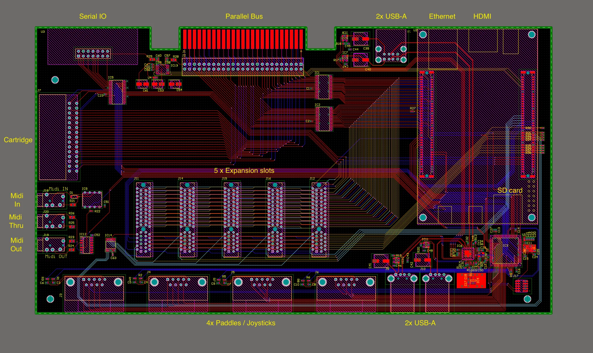
and to pay the gratuitous 3D render tax…
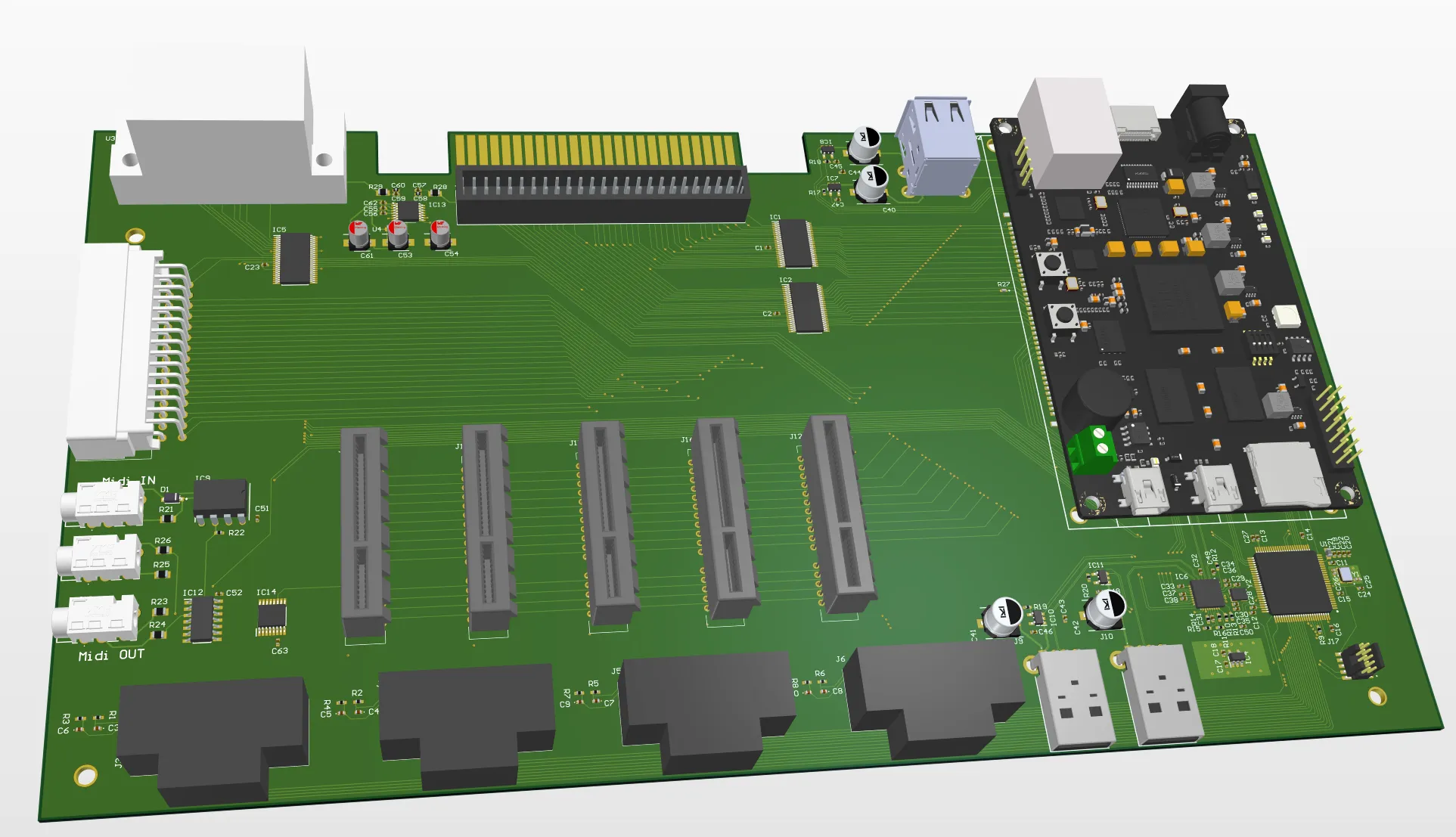
Some minor work remains to be done on the PCB before it’s sent off for production